Introduction: Printed Circuit Boards (PCBs) are the unsung heroes of modern electronic devices, seamlessly connecting components to bring gadgets to life. One crucial element in the PCB manufacturing process that ensures the reliability and functionality of these intricate circuits is the solder mask layer. In this blog post, we will explore the significance of the solder mask layer, its role in PCB design, and why it’s a critical component for electronic reliability.
Understanding the Solder Mask Layer:
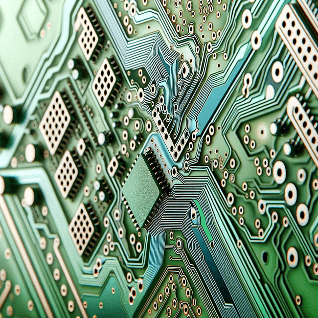
What is a Solder Mask?
The solder mask, also known as solder resist or solder stop mask, is a protective layer applied to the surface of a PCB. This layer serves a dual purpose: to shield the copper traces from environmental factors and prevent unintentional solder bridging during the assembly process.
Environmental Protection:
The solder mask provides a barrier against environmental elements such as dust, moisture, and chemical contaminants. Exposure to these elements can lead to corrosion of the copper traces, compromising the integrity of the circuit. By encapsulating the copper traces, the solder mask enhances the PCB’s durability and longevity.
Prevention of Solder Bridges:
During the soldering process, it’s crucial to ensure that solder only adheres to designated areas. Without the solder mask, there is a risk of solder bridging—unwanted connections between adjacent copper traces. The solder mask prevents these bridges by covering the areas where solder should not be applied, allowing for precise and controlled soldering.
The Composition of Solder Mask:
Materials Used:
Solder masks are typically composed of a polymer-based material; such as epoxy or liquid photoimageable (LPI) solder mask. These materials are applied as a liquid and then cured to form a solid protective layer.
Color Options:
Solder masks come in various colors, with green being the most common. However, other colors, such as red, blue, black, and white, are also available. The choice of color is often based on aesthetic preferences or specific design requirements.
PCB Design and Solder Mask Application:
Design Considerations:
During the PCB design phase, designers must consider the placement of the solder mask layer. Careful attention is given to exposing certain areas for soldering while covering others to prevent unintended connections.
Application Process:
The application of the solder mask involves several steps, including printing, exposure, development, and curing. Modern PCB manufacturing processes often use advanced techniques such as inkjet printing or curtain coating for precise and efficient application.
Conclusion:
In conclusion, the solder mask layer plays a pivotal role in ensuring the reliability and functionality of printed circuit boards. Its protective properties shield PCBs from environmental factors, while its role in preventing solder bridges is crucial for maintaining the integrity of electronic circuits. As technology continues to advance, the importance of the solder mask layer remains paramount in the ever-evolving world of electronics.
For a more in-depth exploration of the solder mask layer and its role in PCB design, check out our comprehensive guide on solder mask. Dive into the intricate details of this essential component and discover how it contributes to the seamless operation of your electronic devices.