Have you ever heard the termPCB, orIntegrated Circuit Board? If you do not know what it is, we will explain it to you in this article. As you read this article, you are surrounded by PCBs; you have several on your PC, monitor, mouse and also on your mobile. Every electronic element is built using a PCB , or at least its “internal organs”.
The use of PCBs was a giant step in the evolution of electronic devices, as it provided an innovative method for connecting elements without using electrical cables . Today’s world would not be the same without the invention of PCBs, so let’s see what they are and how they are made
Also Read: 6 Ways to Find Clients for Your Freelance Business
What is a PCB?

PCB is the acronym for Printed Circuit Board , but we use the acronym in English ( Printed Circuit Board ) so as not to confuse it for example with the PCI slots of our PC.
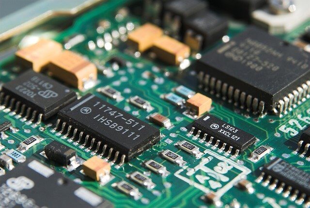
Well, a PCB is basically a physical support where electronic and electrical components are installed and interconnected between them. These components can be, chips, capacitors, diodes, resistors, connectors, etc. If you take a look at a computer inside, you will see that there are multiple flat boards with a lot of components glued to it, it is a motherboard and it is made up of a PCB and the components that we have mentioned
To connect each element on a PCB, we use a series of extremely thin copper conductive tracks that generate a rail, conductor, as if it were a cable. In the simplest circuits, we only have conductive tracks on one or both sides of the PCB, but in more complete ones we have electrical tracks and even components stacked in multiple layers of them.
The main support for these tracks and components is a combination of fiberglass reinforced with ceramic materials, resins, plastic and other non-conductive elements. Although components such as celluloid and conductive paint tracks are currently being used to manufacture flexible PCBs .
The first integrated circuit board was built in 1936 by hand by engineer Paul Eisler to be used by a radio. From there, the processes were automated for large-scale manufacturing, first with radios, and then with all kinds of components.
What is inside a PCB?
Printed circuits are made up of a series of conductive layers , at least the most complex. Each of these conductive layers is separated by an insulating material called a substrate . Holes called vias are used to connect multi-layered tracks, which can go completely through the PCB or only go as far as a certain depth.

external area of the PCBs , and installed on both sides , in order to take full advantage of their extension. Before creating the electrical tracks, the different layers of the PCB are only made up of the substrate and some very thin sheets of copper or other conductive material, and it will be through a machine similar to a printer that these will be created and through a fairly process long and complex.
PCB creation process
We already know what integrated circuit boards are made of, but it would be very interesting to know how they are made . What’s more, we can create a basic integrated circuit ourselves by buying one of these boards, but of course the process will be quite different from the one used in reality
PCB design using software

It all starts with designing the PCB , tracing the electrical tracks necessary to connect the components, as well as listing how many layers are going to be necessary to be able to generate all the connections that are going to be necessary for the components.
This process is carried out using CAM computer software such as TinyCAD or DesignSpark PCB , widely used in engineering careers. Not only are electrical tracks designed, but various labels are also created to list installed components and identify each connector.
All necessary steps in the crafting process will be documented so the manufacturer knows exactly what to do when the project is shipped to you.
Silkscreen and photographic layout
Once designed, we now pass the project directly to the manufacturer and it will be where the physical creation of a PCB begins . The following process is called photographic tracing , whereby a printer-like machine (photoplotter) laser traces a graph with the connection masks of the electronic elements.
For this, a thin sheet of conductive metal of about 7 thousandths of an inch is used. These masks will later serve to determine where the electronic components are glued . In more advanced processes, this process is done directly on the PCB with a printer that engraves the connection masks with this metal.
Inner layer printing

The next thing that is done is the printing on the PCB of the different internal electrical tracks , with a special compound. This involves “painting” a negative of the electrical tracks on the sheet to create a conductive pattern with a photosensitive or dry film material . Well, this film that has been created is exposed to a laser or ultra violet light to remove the excess material and thus create a negative of the final circuit .
This process is performed if the PCB has internal layers with conductive tracks. Furthermore, this process will then be repeated on the outer layers of the PCB to create the final copper tracks and according to the circuit design.
Inspection and Verification (AOI)

Once the different layers of conductive tracks have been made, a machine willinspect that they are all correct and working well. This is done automatically by comparing the original design with the physical print, to search for shorts or broken tracks.
Rust film and lamination
Each of the sheets printed with the conductive tracks undergoes anoxide treatmentto improve the capabilities and durability of the copper tracks of each layer.
Thanks to the process,the delaminationof the different layers and conductive tracks on particularly sensitive PCBs or with a large number of components such as those of computers will be avoided.
The next thing to do isbuild the final PCB, for thiseach of thecircuitlayerswillbe joinedby means offiberglasssheetswith epoxy resin, Pértinaxor any other method used. All this will be perfectly glued by means of ahydraulic pressand this is how we will obtain the integrated circuit board.
Drilling holes

On all occasions we are going to need to make a series ofholesto the PCBs by drillingto be able to join the different copper layers and tracks. We will also need complete perforations to be able to hold electronic elements or different connectors or expansion slots.
The drilling processmust be extremely precise, to preserve the integrity of the PCB, sotungsten carbideheads are used for the hardest material that exists.
Metallic holes
In order for these holes to establish communication with the different internal tracks, aplating processwith a thincopper filmwill be necessary to provide the necessary conductivity. These veneers will be between 40 and 60 millionths of an inch.
The PCB is now ready to trace the copper trackson the outer faces of it.
Outdoor track film and electroplating

Now we willcreate theouterconductive tracks, and for this we will follow the same procedure as to create the internal tracks. First we create thedry film as a negativeof the final circuit. Then, using a laser, the spaces where the copper is going to be deposited are created to create the conductive tracks.
And then the PCB will undergo aelectroplatingprocess , which consists ofgluing the copper in the areas free of dry foil and thus forming the electrical tracks of the PCB. The PCB is placed in a copper bath andelectrolytically bondedto the conductive patterns to create tracks as small as 0.001 inches.
Then another layer of tin will be added ontop of the copper to protect this chemical attack when we go to the SES process or ”strip-etch-strip”
Strip etch strip
This is the penultimate step, the excess copper will be removed from the PCB, the excess will be the one that we have not dipped in tin . In this way, only the copper protected with tin will remain.
Subsequently we must also remove the tin through a chemical treatment to finally leave only the copper tracks that will finally be the ones that will connect components and transport the electricity.
Now another AOI process will verify that everything is correct to finally record the mask and the legend.
Solder mask and legend

Finally, a solder mask will be applied to the electronic circuit board so that later it is possible to solder the components to the tracks correctly and just where they should go.
Then the legend is also printed composite information that the designer wanted to provide the PCB, such as name connectors, code elements, etc . In addition, the final design of the PCB will also be made with the colors that the manufacturer wants to give it, as we see in the gaming motherboards, etc.
Component welding and final tests

The PCB is ready and only the components will be added by means of high precision robot arms, and the corresponding slots. In this way the board is ready to be electrically tested and check that it works correctly.
We will also add the connection masks to weld these elements correctly.
Conclusion and final words
Well this is all about what a PCB is and how they are manufactured. As you can see the process is quite complex and requires many steps, we must bear in mind that the precision must be maximum so that later it works as expected.
PCBs are becoming more complex, with thinner and denser tracks, to be able to house a huge number of components in very little space .